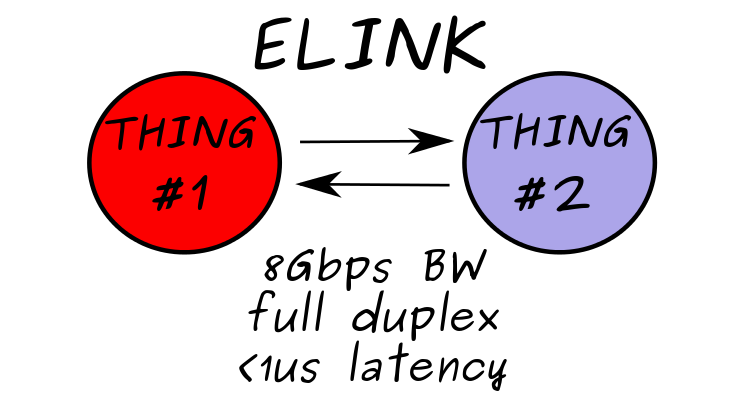
When I created the first Epiphany chip in 2009, I needed a fast low latency interface standard. I couldn’t find one that fit my needs so I created my own. The idea was to move bits between chips at a high rate with minimal overhead.
Design Highlights:
- Everything is a “memory transaction”
- Supports streaming for efficient block transfers
- <1us latency
- 8Gbps peak in modern FPGAs
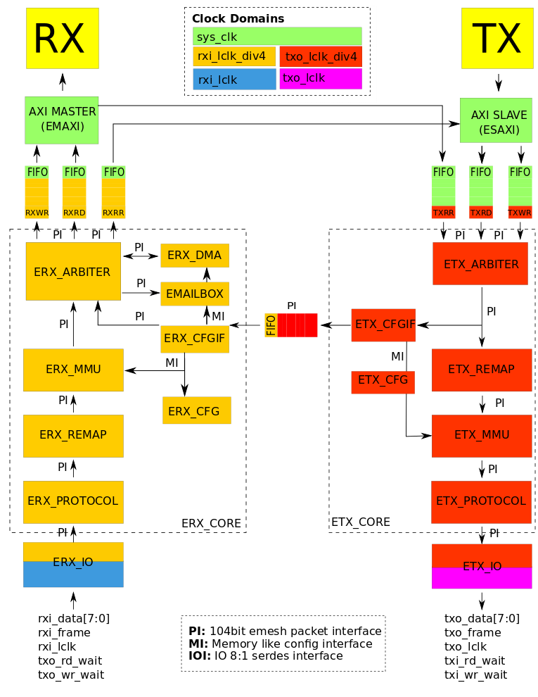
Over the years we used this interface successfully to connect multiple Epiphany chips together and to interface the Epiphany to FPGAs thanks to my friend and colleague Roman Trogan. The design worked well enough but customer handoff was always a struggle and performance was not optimal. Six months ago I set out to completely redesign the FPGA link with the goal of creating a clean elink design that would actually be reusable. The new elink architecture diagram is shown below.
Unfortunately it has been on again off again work due to a lot of other commitments, but I am now quite happy with the state of the design and the block has been successfully tested at a customer. Many thanks goes out to my Swedish friends Gunnar, Patrik, and Jaakko who contributed some of the FPGA related high speed IO black magic to the design! (A second special thanks to Gunnar for pushing me to finally document the behavior of the Epiphany elink properly!)
Full Verilog source code (GPL), testbench and documentation of the new elink interface can be found HERE.
Try it out and let me know what you think. Contributions welcome!
Cheers,
Andreas