[NOTE: this is a community proposal and not part of the official Parallella hardware architecture!]
Introduction
We have a real opportunity to build a thriving expansion board ecosystem for Parallella, with the potential to learn from those that went before it and to advance the state of the art. For this reason I have spent some time thinking about how an expansion system can be built — not just for our applications — that helps resolve the issues highlighted and provides a platform on which a healthy daughter card ecosystem can flourish.
For this post I will be focusing on I/O expansion daughter cards (I will refer to these as Tabs) using just the FPGA PEC and Power PEC, as the Epiphany PECs are part of a very different expansion fabric.
What is required?
So lets take a look at at our fundamental requirements, here are the basic features we require:
- Stackable Tabs: using the third dimension helps us maximise space usage given the relatively small dimensions available for each Tab.
- Cooperative Tabs: one should be able to mix and match several Tabs in any order to provide the application with the resources required to do the job.
- Standardised Tab interfaces: the Tabs themselves must draw on and use standard communication mediums, signals and blocks in order to draw from a common pool of available resources.
- Standard software abstraction: an internal HDL representation and software abstraction in order to interface to each quanta of the input/output fabric.
How do we do it?
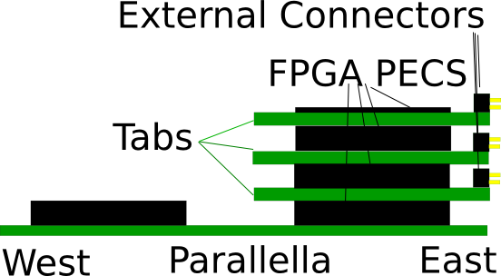
To begin with lets make all Tabs stackable (1) — that means the bottom of each Tab has 2 PEC HTH (PEC FPGA I/O and PEC Power) connectors and 2 PEC HTS connectors aligned on the top and bottom of the Tab PCB. This would allow boards to physically stack on top of each other and signals to be passed through from Tab to Tab in appropriate ways (more on this later).
In terms of signal I/O between the tabs and the real world, external connectors should appear on the east of the board so as not to interfere with Epiphany PEC expansion boards located to the west.
Next lets concern ourselves with Tab coexistence and cooperation (2). This means one should be able to mix different Tabs and even mix several of the same Tabs (for greater capacity) in a Parallella application.
An example
Let’s consider a Parallella Robot example to explore the issues we could encounter in a typical application using such Tabs.
In this example we may require a Camera interface for vision, so lets place a Camera Link Tab first at the bottom of the stack. Next we need to add Motion Control Tab for propulsion and manipulation, and lets assume open loop stepper drivers for this purpose. However, we have a problem: due to dimension limitations the Motion Controller Tabs only support 4 stepper drivers per Tab and we need at least 8 for arms, manipulators and wheels. Thus we need to add 2 Motion Control Tabs. Finally, we need an assortment of inputs for ultrasonic distancing, feeler gauges and ADC measurements etc, so we add a breakout Tab.
We could decide, for example, to allocate certain groups of FPGA I/O pins for specific classes of board. This would enable us to mix a Camera Tab, Breakout Tab and even a Motion Tab safely without conflict. However, if the are multiple identical tabs — and there should be, let’s not reinvent wheel each time — then we will have clashes as the tabs conflict on group pin assignment. Not only that, but we would also leave lots of unused pins and I/O bandwidth because we aren’t using the other classes of tabs to which fixed I/O groups may be reserved.
Introducing Ziports
What would be a better solution here is to start with a pool of standard I/O resources and pick them off as we require them, Tab by Tab. So how can we realise such a design and standard use of limited resources given the available connectors on the on the Parallella board? I’d suggest we use the 48 FPGA I/O lines available as 24 LVDS pairs (actually slightly less as we will likely require a few clocks/strobes to be reserved). These pairs form the quanta and signal path of the standard interface which I shall refer to as Ziports.
A Given Ziport has two selectable and compatible serialiser/deserialiser endpoints: one implemented in HDL on the Zynq, and the other using either an LVDS Ser/Des chip or FPGA on the Tab. Each Ziport once claimed and configured has a fixed direction (input or output) and bit width. The width is determined by the Ziport’s instantiation — it does not change at runtime — and is determined by the Tab and its driver modules and/or definition. This then provides us with standard quanta in which to divide Tab I/O. A Tab therefore will declare how many Ziports it uses and these are fixed.
Tab stacking
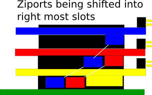
Next we’ll take a look at how we could divide and connect Ziports up in a way that enables the Tabs to be stacked without conflict. I would suggest that we use a technique of shifting the free Ziports as we move up the Tab stack. Here is how that could work physically:
A given Tab uses X number of Ziports from the lowest number pins (think of these a numbered slots containing an LVDS pair) on the PEC connector, then it shifts the remaining free Ziports right onto the lowest Ziport slots (on the next Tab connector), ready for the Tabs above to consume. Each Tab consumes the Ziports it requires from the first (lowest) slots on the PEC connector and in turn shifts the remaining Ziports onto the lowest slots for its next daughter Tab. Think of the interconnects between Tabs as parallel sets of Ziport “escalators” between Tabs, carrying the unused Ziports to the first Ziport slots/pins.
I won’t go into detail about how we could implement the Ziports themselves in this post but will provide an overview of their basic operation and features.
The physical signal across the PEC connectors is LVDS with Ser/Des at each end configured to the required bit width. The output serialiser will have a minimum of two 32 bit registers at the processing end (inside the Zynq FPGA fabric): one for the loadable value of the bit pattern and another which can serialise that bit pattern over LVDS. The deserialiser inputs within the fabric will again have at least two registers, for the received value and a pattern register which can fire events on matching bit patterns during reception. It might later be possible to create simple serial state machine logic as well as the serialiser within the output Ziports, to create all manner of dynamic output bit patterns (timers,waveform generators and tables etc) without requiring extra core cycles to operate them once they are set up. However, I think we would need to keep things fairly simple to begin with, using basic 32 bit register serialisers in order to maintain flexibility, developing more sophisticated state machines as we progress.
We will also need a way to specify Tab configuration, i.e. which Tabs use which Ziports in order to configure and communicate with them at the eCore process end. For this I would suggest we use some sort of file describing the configuration, as this would likely be static.
Basic Ziport operation
Output case
eCore -> Statemachine -> Serialiser -> LVDS -> Deserialiser -> Output
Input case
Input -> Serialiser -> LVDS -> Deserialiser -> Patternmatcher -> eCore
In both cases “Patternmatcher” and “Statemachine” are options. We may also consider DMA source points from Ziport inputs as an additional option for dumping larger IO sequences or frames.
The basic Tab design rule is : consume your required Ziports from the right most slots, shift all remaining unused Ziports into right most slots (think align right for Ziports).
Custom I/O and HDL Tabs
Obviously there is a Ziport configuration default in order to maintain compatibility with between Tabs, but there is nothing preventing custom HDL definition and use of FPGA pins in a other ways as long as it follows the slot shifting rules and doesn’t prevent the remaining unused ports from operating in the standard Ziport manner (i.e. leaving enough resources). That way it allows other Tabs to be mixed with them, cooperating in the Tab ecosystem.
Secondary ports
When Ziports are used by Tabs and the remaining are shifted to lower port slots, spaces are effectively left in the connectors. I can envisage cases where these port spaces may be recycled as a kind of secondary Ziport that is used for inter-tab communication.
Such communications may be used where there is not a requirement eCore processing. This could be pipeline, filtering or hard DSP like applications. Although we would need to explore how this sort of feature could work and be configured.
Conclusion
Using a solution based around Ziports with Tab based shifting, virtual port slots and inter-tab connectors would enable us to create a wealth of cooperative Tabs that could be mixed and matched seamlessly by simply budgeting for the required Ziports. This would work not only for different classes of Tabs but also for multiple Tabs of the same design and class.
Such an approach would support an ecosystem of expansion boards without having to reinvent the wheel each time, providing a catalogue of functionality for diverse applications. Enabling rapid application development based around Parallella boards using skills brought to bare via compatible hardware modules created by the community.
Get involved!
I’m keen to hear your thoughts and have created a forum thread for discussing this further and in order that we can work towards a specification and eventual implementation.
[NOTE: this is a community proposal and not part of the official Parallella hardware architecture!]
great idea. And it looks a bit like the XMOS fancamp is now taking over Parallella… haha 🙂 Good to see you on board, Folknology!
Hey thanks Ozel good to see you on board also. There are bound to be overlaps with the Xmos community given the concurrent nature of both offerings and skill sets within them. I am sure each community will also learn from the other in a positive fashion. Although to be fair each is quite unique in terms of market place positioning and applications.
regards
Al
I can clearly see you put a lot of thought, nothing short of brilliant.
My question is any daughter board can be on top of the stack or buttom of the stack, would that not limit the secondary Ziport (after shifting) that can be used for inter-tab communication to less or equal to the minimum LVDS pair a doughter board must have?
Hi Danny, sorry for the slow reply. To be honest the Secondary Ziports were added at the last minute without much exploration, as a possible use of those empty connector ports created as you move up the stack, so don’t expect this part to be well thought out yet! Clearly with such an idea, secondary ports are considered “secondary” to regular Ziports, filling freed connector slots as they appear. Thus they are more likely to be found towards the top of a stack of tabs rather than the bottom, in terms of availability, they occur in proportion to the consumption of primary Ziports as a secondary effect. This would not prevent a systems designer for example designing a stack of several boards that interoperate together as a set including secondary inter-tab ports. However, once you start breaking the set apart, compatibility with other designer tabs becomes a more complex affair as stack order amongst other things comes into play. I also lack any concrete examples to play around with in order to examine a good use case of secondary Ziports, although Iet us imagine a trivial artificial example:
Perhaps I have a standard cameralink Tab (CL Tab) with a camera attached and I wish to track objects using it. In this case I design an edge detect FPGA DSP Tab which includes secondary Ziports in and Primary Ziports out. This board takes in RGB image data from the Tab above (CL Tab), and outputs monochrome data which represents the edge detect of each frame to the Parallela via Ziports below. In this case the edge detect tab sits inbetween the the CL Tab and the Parallella, effectively presenting secondary Ziports to the CL Tab. It then passes the edge detected monochrome frames over a smaller bandwidth (1 bit vs 16 bit RGB) Ziport to the Parallella (or tabs in the stack below it). In such a manner several image processing tabs could also be inserted as a “stacked pipeline” to sharpen,motion correct or any manner of image processing, leveraging primary and secondary Ziports in a modular fashion. Clearly this is a contrived example and would probably not be a good use case for Parallella as the epiphany cores themselves could actually perform the image processing and edge detect, making such tabs for this purpose would be a little over kill, but I am sure you can see the concept.
What would be a good idea is to start a thread in the daughter card section of the forum (http://forums.parallella.org/viewforum.php?f=11) to kick of a conversation about secondary Ziports so we could actually start covering some of the ideas around them.
I know I haven’t directly answered your question and hope you forgive me, but that is because I hope that your question gets discussed in more detail in a forum thread and hopefully the answers may fall out of that..
regards
Al